SEMICONDUCTORS
Information on Projects Funded to Strengthen U.S. Supply Chain
Report to Congressional Committees
United States Government Accountability Office
A report to congressional committees.
For more information, contact: Candice N. Wright at WrightC@gao.gov.
What GAO Found
As of July 2025, the Department of Commerce has provided incentive awards to 19 companies for 40 projects to construct, expand, or modernize semiconductor facilities. Thirteen of the 19 companies received funding for workforce development activities associated with the projects. In total, Commerce awarded the 19 companies with $30.9 billion in direct funding and two of them with $5.5 billion in loans through the incentive awards.
Commerce awarded projects that collectively aim to address gaps and vulnerabilities at various stages of the supply chain, from materials production to packaging. Nearly 40 percent of projects are intended to produce leading-edge logic chips, which process data for emerging technologies such as artificial intelligence. Commerce estimates that these projects will bring the U.S. share of global leading-edge logic chip manufacturing from 0 percent in 2022 to 20 percent by 2030.
Each project includes unique milestones, which span from November 2024 through October 2033. Commerce officials stated that companies have submitted milestone completion reports for 24 of 161 milestones, as of July 2025. One project, a new leading-edge logic chip manufacturing facility in Arizona, was certified as complete in June 2025.
Note: For more details, see figure 6 in GAO-26-107882.
Officials weighed six criteria to select projects, giving the greatest consideration to projects’ potential impact on economic and national security objectives. For projects selected for an award, officials found that economic and national security benefits outweighed any downsides or risks.
Commerce set award funding amounts to incentivize project completion and distribute funds across a portfolio of projects throughout the supply chain. To ensure that funding amounts would not result in profits that significantly exceed company projections, Commerce negotiated upside sharing agreements for 27 of the 40 projects. Under these agreements, companies share profits with the federal government if their profits exceed a specific threshold.
Why GAO Did This Study
Semiconductors, also called chips, are small electronic devices that are critical to nearly all industries. A global semiconductor shortage occurring from 2020 through 2023 exposed long-term risks in the supply chain. For example, manufacturing facilities are concentrated in a few regions globally.
The William M. (Mac) Thornberry National Defense Authorization Act for Fiscal Year 2021 (as amended, the FY21 NDAA) authorized Commerce to provide financial assistance to entities undertaking semiconductor facility or equipment projects. The CHIPS Act of 2022 appropriated $39 billion for these purposes. In response, Commerce issued the first award in September 2024 after establishing a new office, soliciting input from stakeholders, developing a strategy for the program, and reviewing applications.
The FY21 NDAA also includes a provision for GAO to issue a series of reports on the semiconductor incentives program. This report, the first in the series, examines (1) key characteristics and anticipated timelines of selected projects and (2) how Commerce selected projects and set funding amounts.
This report covers awards made by Commerce from September 2024 through July 2025. GAO analyzed Commerce documents, including notices of funding opportunity, evaluation and selection documents, and awards. In addition, GAO reviewed relevant requirements in the FY21 NDAA and compared Commerce’s efforts to those requirements. GAO also interviewed Commerce officials.
Abbreviations
ATP assembly, testing, and packaging
CHIPS Act CHIPS Act of 2022
DOD Department of Defense
FY21 NDAA William
M. (Mac) Thornberry National Defense
Authorization Act for Fiscal Year 2021, as
amended
R&D research and development
This is a work of the U.S. government and is not subject to copyright protection in the United States. The published product may be reproduced and distributed in its entirety without further permission from GAO. However, because this work may contain copyrighted images or other material, permission from the copyright holder may be necessary if you wish to reproduce this material separately.
December 11, 2025
Congressional Committees
Semiconductors, also called chips, are small electronic devices that are critical to nearly all industries. A global semiconductor shortage occurred from 2020 through 2023. The shortage affected multiple sectors, including the automotive and medical equipment industries, as well as the broader U.S. economy. It also exposed long-term risks in the supply chain, such as potential choke points resulting from the concentration of raw materials and manufacturing facilities in a few regions globally. Given these risks and a declining U.S. share of global production, policymakers have expressed concerns about future supply chain reliability and security.
The William M. (Mac) Thornberry National Defense Authorization Act for Fiscal Year 2021 (as amended, the FY21 NDAA) authorizes the Department of Commerce to provide financial assistance to entities undertaking projects to construct, expand, or modernize semiconductor-related facilities or equipment. The FY21 NDAA includes specific requirements for eligible entities and projects.[1] The CHIPS Act of 2022 (CHIPS Act) appropriated $39 billion for these purposes.[2]
The FY21 NDAA also includes a provision for GAO to issue a series of reports on the semiconductor incentives program.[3] This report, the first in the series, examines (1) key characteristics and anticipated timelines of projects selected for incentive awards and (2) how Commerce selected projects and set funding amounts. Later products will cover project outcomes and the semiconductor industry workforce, among other topics.
Our scope includes incentive awards made by Commerce for manufacturing and other activities under Section 9902 of the FY21 NDAA from September 2024 through July 2025.[4] Information in this report does not include any award amendments made after July 2025. For example, in August 2025, Commerce amended the award agreement for one award recipient’s six projects.[5] We have included information on those awards as of July 2025, but this information is subject to change based on the amendments.
To address both of our objectives, we analyzed Commerce documents, including notices of funding opportunity, evaluation and selection documents, and awards. We analyzed Commerce information using data collection instruments to summarize evaluation, selection, and award documents. In addition, we reviewed relevant requirements in the FY21 NDAA and compared Commerce’s efforts to these requirements. We also interviewed Commerce officials.
We conducted this performance audit from October 2024 to December 2025 in accordance with generally accepted government auditing standards. Those standards require that we plan and perform the audit to obtain sufficient, appropriate evidence to provide a reasonable basis for our findings and conclusions based on our audit objectives. We believe that the evidence obtained provides a reasonable basis for our findings and conclusions based on our audit objectives.
Background
Semiconductors
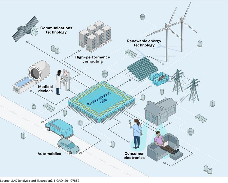
Nearly all industries rely on semiconductors because they are critical components of digital technologies (see fig. 1). Chips are generally smaller than postage stamps yet contain billions of components that control the flow of electric current to store, process, or move data.
Types
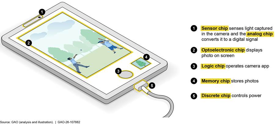
Different types of chips perform different functions and are found in various end products (see table 1). Two types, logic and memory, accounted for approximately 60 percent of global semiconductor sales in 2024, according to information from one industry group.[6]
|
Type |
Function |
Example end products |
|
Logic |
Process information |
Computers, phones, other smart devices |
|
Memory |
Store information |
Computers, flash drives, phones, data centers |
|
Analog |
Convert analog and digital information |
Military surveillance equipment, medical devices |
|
Optoelectronic |
Interact with or produce light |
Light emitting diodes |
|
Sensor |
Detect or control properties (e.g., pressure) |
Vehicles, industrial equipment, weather sensors |
|
Discrete |
Perform a single function (e.g., electrical flow) |
Power supplies, amplifiers |
Source: GAO. | GAO‑26‑107882
Many products contain multiple types of chips (for example, see fig. 2).
Nodes
Semiconductor technology has matured over several decades, with more advanced chips typically offering higher performance in less physical space. Chips are classified into three levels of maturity—referred to as nodes:[7]
· Leading-edge. Leading-edge nodes are produced using the most advanced manufacturing processes and are fundamental to emerging technologies, such as artificial intelligence. They are typically logic and memory chips.
· Current generation. Current generation nodes support a wide range of modern technologies, including numerous consumer products. They include various chip types.
· Mature. Mature nodes are produced using less advanced manufacturing processes. However, they are still in high demand within the automotive and health care industries, and in end products with long lifespans, such as those used in critical infrastructure and defense systems. Mature nodes include logic, analog, optoelectronic, sensor, and discrete chips.
Production Stages
Semiconductor production involves three broad stages: (1) design; (2) wafer and chip manufacturing; and (3) assembly, testing, and packaging (ATP); as shown in figure 3. Manufacturing and ATP both require specialized equipment and many different raw materials. Different companies based in multiple countries produce the equipment and materials, which introduces complexity to the supply chain. In addition, all three stages continue to evolve through advancements in research and development (R&D).
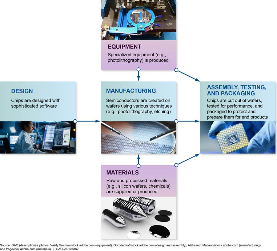
The semiconductor industry has changed over time as technology has advanced. Historically, companies performed all three stages in-house. However, as chip design and manufacturing became more complex, companies began specializing. The U.S. is the world leader in the design stage, with the highest market share and the most facilities. Many U.S. companies focus on designing chips and contract with other companies to manufacture them in facilities called foundries. In addition, some companies complete the ATP stage at their own facilities, while others outsource it.
Supply Chain Gaps and Vulnerabilities
The U.S. faces key gaps and vulnerabilities that affect the resilience of the semiconductor supply chain.[8] Two key issues related to supply chain gaps and vulnerabilities are geographic concentration and declining domestic capacity.[9]
First, about three-quarters of chips were manufactured and packaged in Asia as of 2022.[10] Manufacturing for certain chip types, such as logic and memory chips, is particularly concentrated in Taiwan and South Korea. When industries are geographically concentrated rather than diversified, problems in one location (e.g., geopolitical conflicts, trade disputes, natural disasters) can disrupt the supply chain.
Second, U.S. semiconductor production capacity has declined in recent decades. According to an industry report, the U.S. share of global capacity dropped from 37 percent in 1990 to 10 percent in 2022.[11] In addition, the report found that the U.S. did not produce any leading-edge logic chips at commercial scale and produced only 3 percent of the two most common types of memory chips as of 2022.[12]
Increasing domestic capacity is challenging for several reasons:
· Construction costs. Constructing a new facility, including labor and utilities, can cost several billion dollars. These costs can be lower in some foreign countries, in part, because those countries’ governments have invested in their semiconductor industries for decades.
· Construction timeframes. A single new facility can take 2 to 5 years to become operational, based on regulatory approvals (e.g., permits), construction, utility connections, and equipment installation.[13] This can present a challenge to building new facilities quickly in response to changes in demand—incentivizing reliance on existing production facilities.
· Workforce needs. Semiconductor manufacturing requires a specialized workforce, including engineers, technicians, and computer scientists. A July 2023 industry report estimated that over half of the projected semiconductor industry job growth by 2030 may go unfilled, based on U.S. education rates at that time.[14]
Limited domestic semiconductor capacity could dampen U.S. economic and national security interests. It could hamper innovation, especially for emerging technologies, and it presents risks to a secure supply of semiconductors for critical industries. For example, the Department of Defense (DOD) uses current generation and mature chips to maintain existing weapons systems. Relying on other countries, such as China, to supply these chips could present national security risks.
Semiconductor Incentives Program Requirements
FY21 NDAA and CHIPS Act
The FY21 NDAA created several programs to address gaps and vulnerabilities in the supply chain, including the semiconductor incentives program.[15] For the semiconductor incentives program, the Secretary of Commerce must select projects that bolster U.S. economic and national security interests and must ensure that assistance supports multiple nodes.[16] Under the act, Commerce may provide direct funding, loans, or loan guarantees.[17]
The FY21 NDAA contains several eligibility requirements for the program. Awardees may be headquartered outside the U.S., but they must use funds for facilities inside the U.S.[18] In addition to supporting the construction of facilities, funding may also support the production of equipment and materials. Awardees may also use funding to support workforce development activities for eligible facilities.[19]
Further, the act requires the Secretary of Commerce to implement certain guardrails to protect federal investment in projects.[20] Awardees that fail to meet statutory guardrails, such as target dates for starting and completing projects, are subject to clawbacks under which the federal government may recover funding.
Department of Commerce
Commerce’s National Institute of Standards and Technology is responsible for implementing the semiconductor incentives program. In response to the FY21 NDAA, Commerce established the CHIPS Program Office to administer the program.[21] It released a request for information in January 2022 seeking stakeholder perspectives to help inform the planning and design of the program.
Commerce then published an overall strategy document in September 2022, as well as two vision documents to define specific aspects of the program in February and June 2023.[22] These documents include goals for the program. For example, one goal is to make large-scale investments in leading-edge logic and memory chip manufacturing in regional clusters. Another is to expand capacity for current generation and mature nodes, new and specialty technologies, equipment, and materials.
Commerce released notices of funding opportunity in February and September 2023. The first notice was for all projects for wafer and chip manufacturing and ATP, and for projects producing semiconductor materials or equipment with total capital expenditures greater than or equal to $300 million. The second was for semiconductor materials or equipment projects with capital expenditures less than $300 million.
These notices describe eligible projects, information that applicants must provide, and Commerce’s process and criteria for selecting projects. For example, the first notice stated that Commerce would first review applications and prepare nonbinding preliminary terms for selected projects. Officials would then conduct additional analyses and negotiate terms with applicants before deciding whether to make final awards.
Awarded Projects Aim to Help Strengthen the U.S. Supply Chain but Will Take Years to Complete
Commerce Has Selected 40 Projects for Incentive Awards
Between September 2024 and July 2025, Commerce made incentive awards to 19 companies for 40 total projects (see table 2). All of the selected projects are in response to the first notice of funding opportunity. The first notice was for all projects for wafer and chip manufacturing and ATP, and for projects producing semiconductor materials or equipment with total capital expenditures greater than or equal to $300 million.
These projects were selected from 103 applications that companies submitted, according to Commerce officials.[23] Commerce provided awards for most of the projects through January 2025 but provided awards for two additional projects in June 2025.[24]
All 19 companies received direct funding (totaling $30.9 billion), and two also received loans (totaling $5.5 billion). The $30.9 billion includes $30.6 billion in funding for the 40 projects to construct, expand, or modernize facilities. It also includes $296 million that 13 companies received for workforce development activities associated with their projects.
The direct funding awards represent 89 percent of the $34.7 billion in available funds for direct funding.[25] As of July 2025, Commerce officials stated that they are in the process of reviewing additional applications received.
|
|
|
Funding amount (in millions) |
|
||
|
Awardee |
Number of projects |
Direct funding |
Loans |
Total |
Percentage of all funding awarded |
|
Taiwan Semiconductor Manufacturing Company |
3 |
$6,565 |
$5,000 |
$11,565 |
31.7% |
|
Intel |
6 |
$7,865 |
— |
$7,865 |
21.6% |
|
Micron |
5 |
$6,440 |
— |
$6,440 |
17.7% |
|
Samsung |
4 |
$4,745 |
— |
$4,745 |
13.0% |
|
Texas Instruments |
3 |
$1,610 |
— |
$1,610 |
4.4% |
|
GlobalFoundries |
3 |
$1,587 |
— |
$1,587 |
4.4% |
|
SK hynix |
1 |
$458 |
$500 |
$958 |
2.6% |
|
Amkor Technology |
1 |
$407 |
— |
$407 |
1.1% |
|
GlobalWafers |
2 |
$406 |
— |
$406 |
1.1% |
|
Hemlock Semiconductor |
1 |
$325 |
— |
$325 |
0.9% |
|
Polar Semiconductor |
1 |
$123 |
— |
$123 |
0.3% |
|
Infineraa |
2 |
$93 |
— |
$93 |
0.3% |
|
Entegris |
2 |
$77 |
— |
$77 |
0.2% |
|
Absolics |
1 |
$75 |
— |
$75 |
0.2% |
|
HP |
1 |
$53 |
— |
$53 |
0.1% |
|
BAE Systems |
1 |
$36 |
— |
$36 |
0.1% |
|
Corning |
1 |
$32 |
— |
$32 |
0.1% |
|
Rocket Lab (SolAero) |
1 |
$24 |
— |
$24 |
0.1% |
|
Edwards |
1 |
$18 |
— |
$18 |
0.05% |
|
Total |
40 |
$30,938 |
$5,500 |
$36,438 |
100% |
— = None received
Source: GAO analysis of Department of Commerce documents. | GAO‑26‑107882
Note: Awards are authorized under Section 9902 of the William M. (Mac) Thornberry National Defense Authorization Act for Fiscal Year 2021, as amended. The table does not include awards made under the Secure Enclave program. Funding amounts also include funding for workforce development activities associated with the projects. Amounts are rounded to the nearest million dollar, and percentages are rounded to the nearest tenth of a percent or first significant digit.
aInfinera was acquired by Nokia in February 2025.
Awards only cover a portion of the projects’ total expected capital expenditures, ranging from 4.6 to 38.8 percent, with a median of 14.2 percent (see fig. 4). Companies must make their own investments or seek additional nonfederal investments to cover the remainder of expenditures.
Figure 4: Semiconductor Incentive Facility Funding as a Percentage of Projected Capital Expenditures, as of July 2025
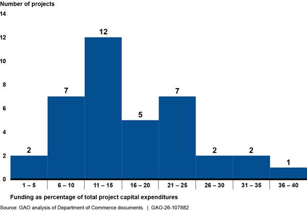
Note: Awards are authorized under Section 9902 of the William M. (Mac) Thornberry National Defense Authorization Act for Fiscal Year 2021, as amended. Projected capital expenditures are estimated by companies. Percentages are rounded to the nearest 1 percent. Forty total projects received funding. However, capital expenditure data for three projects from the same company were only available combined. We treated those three projects as one project for the purposes of the figure. The figure does not reflect award amendments made after July 2025, such as an August 2025 amendment to the award agreement for six of the 40 projects.
The projects are located in 19 states. Arizona, New York, and Texas account for half of the projects (20 of 40) and nearly three-quarters of facility funding ($26.7 billion of $36.4 billion). One of Commerce’s goals for the incentives program was to establish at least two new large-scale clusters of leading-edge logic chip manufacturing facilities.[26] Projects in these three states were among those that received funding for such facilities. See figure 5 for a map of all project locations and appendix I table 4 for a complete list of projects.
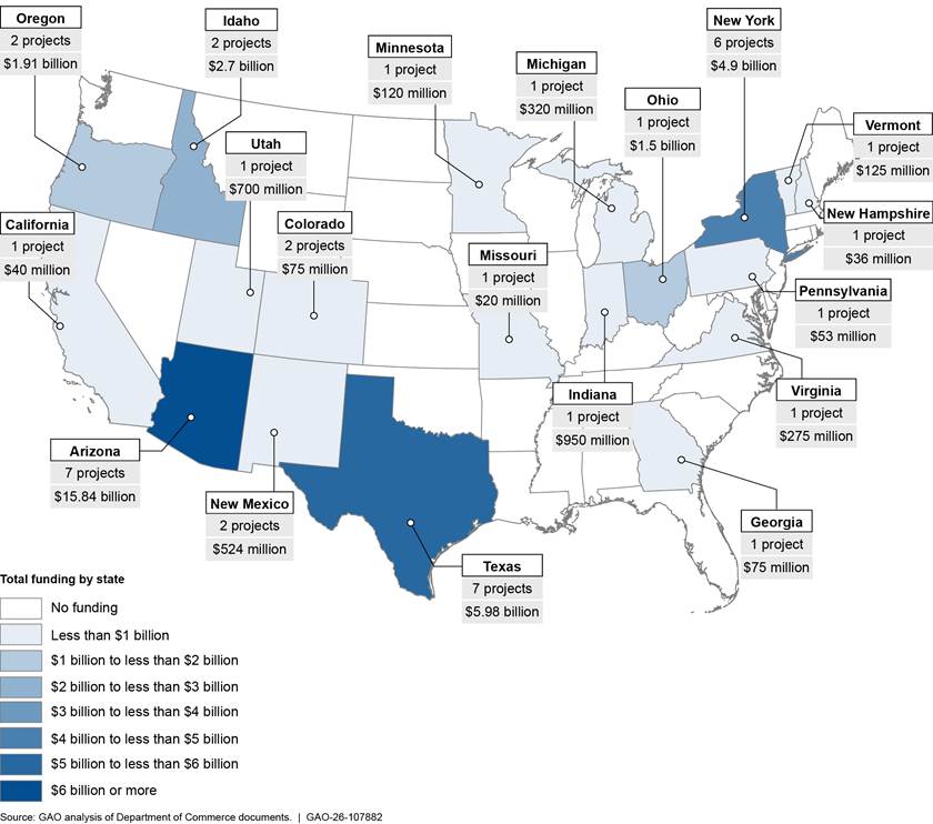
Note: Awards are authorized under Section 9902 of the William M. (Mac) Thornberry National Defense Authorization Act for Fiscal Year 2021, as amended. Funding is rounded to the nearest $1 million. The figure does not reflect award amendments made after July 2025, such as an August 2025 amendment to the award agreement for six projects in Arizona, New Mexico, Ohio, and Oregon.
Projects Aim to Help Address Gaps and Vulnerabilities Across the U.S. Supply Chain
Commerce awarded projects that collectively aim to help address existing gaps and vulnerabilities at most stages of the supply chain, according to our analysis of Commerce’s application evaluation and award documents. The 40 projects support wafer or chip manufacturing, ATP, materials production, or equipment production. Seven of the 40 projects span multiple stages.
Wafer and Chip Manufacturing
Four-fifths of projects (32 of 40) involve wafer or chip manufacturing. These projects are expected to produce a range of chip types across various nodes (see app. I table 5). Projects producing leading-edge logic chips are the most common (15 of 32 manufacturing projects). However, Commerce also funded a wide range of other projects, including for mature nodes, as required in the FY21 NDAA.[27]
The wafer and chip manufacturing projects are expected to help advance geographic diversity and domestic capacity. For example, the leading-edge logic projects will be the first of their kind in the U.S. and outside of Asia. Commerce estimates that these projects will bring the U.S. share of global leading-edge logic chip manufacturing from 0 percent in 2022 to 20 percent by 2030.[28] These projects are also expected to create thousands of facility and construction jobs. For example, according to a Commerce document, one company’s projects are estimated to create more than 14,000 jobs over 2 decades.
Assembly, Testing, and Packaging
One-fifth of projects (8 of 40) involve the ATP stage. Some projects are expected to support ATP of specific chip nodes and types, whereas others support all nodes and types. See appendix I table 6 for descriptions of each project.
According to Commerce documents, awarded projects are expected to help establish U.S. leadership in advanced packaging.[29] The U.S. held about one-quarter of the global share of advanced packaging as of 2020.[30] Advanced packaging comprises various innovative techniques to connect and improve communication between chips. It has become an increasingly important method of increasing chip performance as the rate of chip miniaturization slows.[31]
Materials and Equipment
Five of 40 projects involve the production of materials or equipment used in semiconductor manufacturing. All of these projects are expected to support chips of all nodes and types. See appendix I table 7 for descriptions of each project.
These projects are expected to help advance domestic capacity and U.S. technology leadership. For example, one project will create the first dry vacuum pump production facility in the U.S. These pumps are necessary for all semiconductor manufacturing facilities but are vulnerable to tampering, which could shut down entire production lines. Producing them domestically would strengthen supply chain security. Once fully operational, Commerce expects the project to meet demand for all existing and projected U.S. facilities over the next several years.
Workforce
In addition to facilities, incentive awards fund workforce development activities associated with 13 companies’ projects. Workforce activities aim to fill gaps in the regional labor supply (e.g., engineers, technicians, construction workers) to ensure successful execution of projects. Some are intended to develop a sustainable workforce, such as funding K-12 and postsecondary programs to increase the pipeline of skilled workers. Some companies have identified academic or nonprofit partners, such as local economic development organizations, to serve as intermediaries for training.
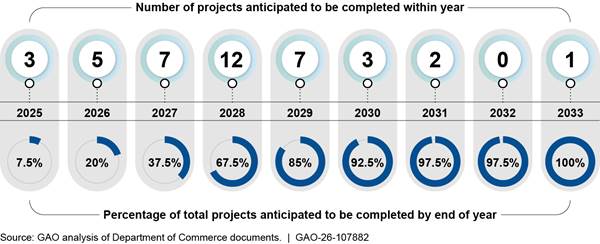
Milestones for Project Completion Extend to 2033
Each project includes unique project milestones, which span from November 2024 through October 2033 (see fig. 6), according to our analysis of Commerce award documents.
Figure 6: Semiconductor Incentive Award Facility Projects’ Anticipated Completion Dates, as of July 2025
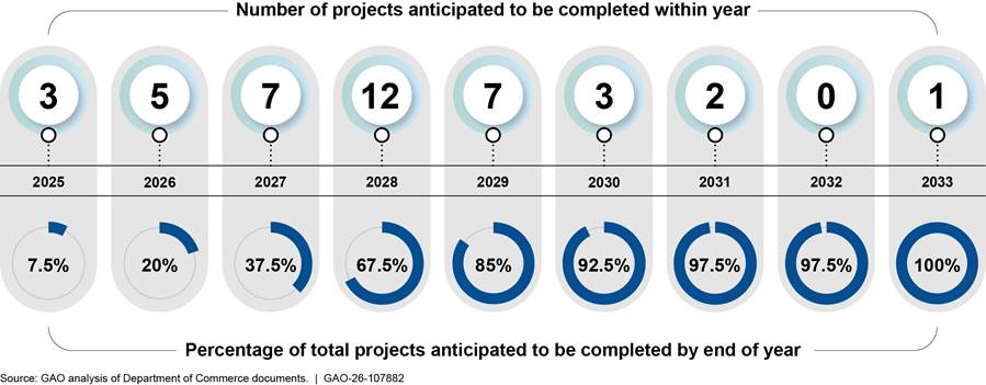
Note: Awards are authorized under Section 9902 of the William M. (Mac) Thornberry National Defense Authorization Act for Fiscal Year 2021, as amended. The figure does not reflect award amendments made after July 2025, such as an August 2025 amendment to the award agreement for six projects.
Commerce award documents identify 161 total milestones across the 40 projects. The milestones relate to construction of facilities, installation and qualification of equipment, and meeting minimum production levels. For example, one project has four milestones with anticipated completion dates on roughly an annual basis from 2027 to 2031.
Commerce officials stated that companies have submitted reports of milestone completion for 24 of 161 milestones, as of July 2025. One project, a new leading-edge logic chip manufacturing facility in Phoenix, Arizona, which started construction prior to the enactment of the CHIPS Act according to information on the company’s website, was certified as complete in June 2025. The company received a $2.9 billion award for the project. Commerce also received 11 requests for disbursements for workforce activities. As of July 2025, Commerce has reviewed and verified completion of 18 of 35 disbursement requests, and it has disbursed $6 billion. Officials stated that they are still reviewing reports for the remaining 17 disbursement requests.
Commerce disburses funding to awardees after proof of milestone completion, according to officials. Disbursements are in effect reimbursements to companies, which front the project costs until milestones are completed. If companies do not complete certain milestones and other terms, Commerce may require partial or full repayment of funds previously disbursed, referred to as clawbacks.
Commerce Conducted Extensive Analyses to Select Projects and Set Funding Amounts
Commerce Weighed Multiple Criteria Using Applicant-Provided and Independently Collected Information to Select Projects
Commerce officials weighed six criteria (see table 3), using applicant-provided and independently collected information, to select projects for incentive awards, according to our analysis of Commerce documents.
|
Criterion |
Examples of information considered |
|
Potential impact on economic and national security objectives |
· Potential to advance supply chain resilience and domestic capacity · Potential to support national security needs and supply chain security |
|
Commercial viability |
· Customer base, including size, strength, relationships, and likelihood of adopting new technologies · Customer commitments (e.g., advance orders and payments) · Product and end-market demand · Competitive advantages |
|
Financial strength |
· Market share and profit performance · Private capital investments · Debt and cash flows · Credit risk |
|
Technical feasibility and readiness |
· Operational readiness (e.g., logistics experience) · Supplier network · Construction plans · Regulatory compliance (e.g., permitting) progress |
|
Workforce development |
· Recruitment and hiring plans · Employee training and education · Employee services (e.g., parental leave and childcare) · Employee health and safety procedures |
|
Broader impacts |
· Community investments (e.g., housing and transportation) · Plans to engage small or disadvantaged suppliers and contractors · Investments in research and development · Participation in federally funded research and development partnerships |
Source: GAO analysis of Department of Commerce documents. | GAO‑26‑107882
Note: Awards are authorized under Section 9902 of the William M. (Mac) Thornberry National Defense Authorization Act for Fiscal Year 2021, as amended. Criteria are for the first notice of funding opportunity, which was released in February 2023 and revised in June 2023. The table does not address criteria for awards made under the Secure Enclave program.
Of the six criteria, Commerce gave greatest consideration to projects’
potential impact on economic and national security objectives in alignment with
FY21 NDAA requirements.[32]
· Economic security. Commerce considered the potential for projects to advance supply chain resilience and domestic production capacity. Regarding supply chain resilience, officials analyzed factors such as projects’ potential to improve geographic diversity, particularly for chip types produced primarily in Asia. Regarding domestic capacity, officials analyzed various factors such as the potential to maintain or establish U.S. technology leadership. For example, Commerce selected one project that could establish the U.S. as the first country to adopt a new advanced technology. The technology is expected to result in 40 to 50 percent improvements in performance, manufacturing time, and costs, according to a Commerce document.
Commerce also considered the potential for projects to support advancements in critical industries, such as communications, information technology (e.g., artificial intelligence, data centers, high-performance computing), and transportation.
Further, for larger proposed awards, Commerce considered whether projects could create jobs and advance regional technology ecosystems. According to Commerce documents, large projects could attract suppliers and other new entities to the area. All of the projects may also collaborate with existing regional consortia, such as Tech Hubs and Microelectronics Commons Hubs.[33]
· National security. Commerce considered the potential for projects to support national security. This included determining whether the resulting technology would be used in specific defense systems or meet immediate DOD needs, and considering applicants’ history working with the defense industrial base. For example, Commerce selected a project anticipated to quadruple production for DOD customers and also provide greater reliability and increased delivery speed. In some cases, successful applicants agreed to certain commitments to DOD, such as priority access to critical technologies. Commerce also considered whether applicants had participated in the DOD Trusted Foundry program, obtained facility security clearances, or conducted classified work.[34]
In addition, Commerce considered national security risks. To assess these risks, officials analyzed foreign ties, supplier networks, and cybersecurity procedures, among other factors. Commerce also considered whether the projects may mitigate existing risks. For example, officials found that some applicants’ competitors are based in China, so the projects could reduce reliance on Chinese goods.
Commerce officials reviewed information that companies provided in their applications. Applicants were required to include specific information, in alignment with the FY21 NDAA and the notice of funding opportunity. The FY21 NDAA requires that applicants disclose security risks, identify potential customers, demonstrate means to financially sustain funded facilities, develop workforce strategies, and make commitments to community investments, among other requirements.[35] In addition, the notice of funding opportunity required applicants to include detailed information such as supply chain maps.
To corroborate and supplement information that applicants provided, Commerce also independently collected information from available datasets, site visits, interviews with potential customers, or input from DOD. For example, officials analyzed data on demand trends for semiconductor products, as well as demand in end markets that use the products (e.g., electric vehicles). In some cases, Commerce hired third-party consultants to analyze a range of topics, from construction to tax compliance.
Further, Commerce collected information on any parent companies and analyzed the likelihood that parent companies would support projects that had been awarded funding. For example, officials examined the extent of parent company investment in applicants. Officials also assessed whether parent companies were economically incentivized to support projects or had made agreements to do so, such as through debt guarantees. Beyond financial support, Commerce also considered whether the parent company would provide operational support. For example, officials determined whether parent companies had shared supplier and customer networks with applicants. Access to these networks could help applicants identify viable suppliers and customers more quickly.
To assess information against criteria, Commerce weighed benefits with downsides and risks. For projects selected for award, officials found that economic and national security benefits outweighed any downsides or risks. For example, officials identified early-stage commercialization risks for a project producing a new technology. Specifically, customers may be slow to adopt a new technology into their existing processes. However, Commerce determined that such risks are inherent to investing in new technology. Thus, officials selected the project, conditional on the applicant taking steps to mitigate risks. For projects denied an award, Commerce either found that benefits did not outweigh downsides or risks, or that the project was not eligible for an award.
Commerce Set Funding Amounts to Incentivize Completion of a Portfolio of Projects
We found that Commerce set award funding amounts to incentivize completing projects and distribute funds across a portfolio of projects, based on our analysis of agency documents.
Incentives for Project Completion
According to agency documents, Commerce sought to set award funding amounts that would address project financial needs and ensure completion, while also limiting each award amount to protect taxpayer dollars. Specifically, officials determined the award amount needed to generate sufficient profit to incentivize the applicant to invest its own resources in the project.[36] This analysis accounted for several factors, including
· the Advanced Manufacturing Investment Credit, a federal tax incentive for eligible projects;[37]
· state and local grants, loans, and tax incentives; and
· risks to company profits, such as geopolitical uncertainties.
Commerce documents state that officials aimed to ensure that awarded projects would be completed. While Commerce may be able to recover funds for terminated projects through clawback provisions, reinvesting funds in other projects would entail additional time and costs.
In some cases, Commerce also considered whether increased funding amounts would result in federal cost savings. In particular, DOD provided input to Commerce that investing in certain projects would effectively lower prices for DOD procurement. For example, one company’s award could result in measurable improvements in scale, yield, and time to meet DOD semiconductor needs. According to a Commerce document, DOD has existing agreements with the company that prices for DOD are set at a specific mark-up above per-unit cost. Through pre-award negotiations with the company, Commerce sought to ensure that production improvements, if realized, would result in lower prices for DOD. The Commerce document states that both Commerce and DOD will audit any improvements to ensure that they translate to lower prices.
To ensure that funding amounts would not result in profits that significantly exceed company projections, Commerce negotiated upside sharing agreements with some companies. Under these agreements, companies share profits with the federal government if their profits exceed a specific threshold. Commerce obtained upside sharing agreements for 27 of the 40 awarded projects. These 27 projects had a higher median award amount ($825 million) compared to the 13 without upside sharing agreements ($40 million). The notice of funding opportunity states that upside sharing agreements would be required for all projects receiving greater than $150 million in direct funding, with limited exceptions. The purpose of upside sharing is not to regulate or reduce commercial profits but rather to incentivize companies to provide reasonable profit projections that will help inform appropriate award amounts, according to information provided with the notice of funding opportunity. Without such agreements, companies may be incentivized to underestimate projected profits in order to seek larger awards. Under the agreements, if companies underestimate profits too much, they may have to pay out a portion of profits later. Thus, upside sharing agreements may result in more accurate upfront profit projections.
Upside sharing agreements varied. The first profit threshold at which a project’s upside sharing agreements would go into effect ranged from approximately $3 million to $29.2 billion, with a median of $7.7 billion.[38] Percentage of profit to be shared with the federal government ranged from approximately 2 percent to 31 percent, with a median of 22 percent.[39] However, Commerce has stated that upside sharing is generally not expected to occur, because thresholds are significantly above projected profits.
Distribution of Funding Across a Portfolio of Projects
Commerce documents stated that officials examined funding amounts as a percentage of total program funds to ensure availability of program funds for a portfolio of projects across the supply chain. The first notice of funding opportunity stated that direct funding awards would generally cover 5 to 15 percent of capital expenditures, and all awards (including the principal amount of loans and loan guarantees) would generally cover up to 35 percent.[40] Commerce documents state that officials generally aimed to keep funding amounts within these ranges. Documents stated that Commerce sought to avoid the appearance that some companies unfairly received larger awards than others. One project received funding for greater than 35 percent of estimated capital expenditures, but Commerce documents state that this was primarily because the project has potential national security benefits and is not eligible for tax incentives from the Advanced Manufacturing Investment Credit. In addition, Commerce aimed to ensure that it distributed funding across a portfolio of projects by not providing more than $3 billion for any individual project, as called for by the FY21 NDAA.[41]
Agency Comments
We provided a draft of this report to the Department of Commerce for review and comment. Commerce provided technical comments, which we incorporated as appropriate.
We are sending copies of this report to the appropriate congressional committees, the Secretary of Commerce, and other interested parties. In addition, the report is available at no charge on the GAO website at https://www.gao.gov.
If you or your staff have any questions about this report, please contact me at WrightC@gao.gov. Contact points for our Offices of Congressional Relations and Public Affairs may be found on the last page of this report. GAO staff who made key contributions to this report are listed in appendix II.

Candice N. Wright
Director, Science, Technology Assessment, and Analytics
List of Committees
The Honorable Susan Collins
Chair
The Honorable Patty Murray
Vice Chair
Committee on Appropriations
United States Senate
The Honorable Roger Wicker
Chairman
The Honorable Jack Reed
Ranking Member
Committee on Armed Services
United States Senate
The Honorable Tim Scott
Chairman
The Honorable Elizabeth Warren
Ranking Member
Committee on Banking, Housing, and Urban Affairs
United States Senate
The Honorable Ted Cruz
Chairman
The Honorable Maria Cantwell
Ranking Member
Committee on Commerce, Science, and Transportation
United States Senate
The Honorable Mike Lee
Chairman
The Honorable Martin Heinrich
Ranking Member
Committee on Energy and Natural Resources
United States Senate
The Honorable Mike Crapo
Chairman
The Honorable Ron Wyden
Ranking Member
Committee on Finance
United States Senate
The Honorable James E. Risch
Chairman
The Honorable Jeanne Shaheen
Ranking Member
Committee on Foreign Relations
United States Senate
The Honorable Rand Paul, M.D.
Chairman
The Honorable Gary C. Peters
Ranking Member
Committee on Homeland Security and Governmental Affairs
United States Senate
The Honorable Tom Cotton
Chairman
The Honorable Mark Warner
Vice Chairman
Select Committee on Intelligence
United States Senate
The Honorable Tom Cole
Chairman
The Honorable Rosa DeLauro
Ranking Member
Committee on Appropriations
House of Representatives
The Honorable Mike Rogers
Chairman
The Honorable Adam Smith
Ranking Member
Committee on Armed Services
House of Representatives
The Honorable Brett Guthrie
Chairman
The Honorable Frank Pallone, Jr.
Ranking Member
Committee on Energy and Commerce
House of Representatives
The Honorable French Hill
Chairman
The Honorable Maxine Waters
Ranking Member
Committee on Financial Services
House of Representatives
The Honorable Brian Mast
Chairman
The Honorable Gregory Meeks
Ranking Member
Committee on Foreign Affairs
House of Representatives
The Honorable Andrew Garbarino
Chairman
The Honorable Bennie G. Thompson
Ranking Member
Committee on Homeland Security
House of Representatives
The Honorable Brian Babin
Chairman
The Honorable Zoe Lofgren
Ranking Member
Committee on Science, Space, and Technology
House of Representatives
The Honorable Jason Smith
Chairman
The Honorable Richard Neal
Ranking Member
Committee on Ways and Means
House of Representatives
The Honorable Rick Crawford
Chairman
The Honorable Jim Himes
Ranking Member
Permanent Select Committee on Intelligence
House of Representatives
The Department of Commerce made semiconductor incentive awards for 40 projects, as of July 2025 (see table 4). The 40 projects are to construct, expand, or modernize facilities. In addition, 13 companies received funding for workforce development activities associated with the projects.
|
Project or activity |
Total direct funding and loan amount |
Location |
|
Absolics Georgia |
$75,000,000 |
Covington, Georgia |
|
Amkor Arizona |
$400,000,000 |
Peoria, Arizona |
|
Amkor Arizona Workforce |
$7,000,000 |
Peoria, Arizona |
|
BAE Systems New Hampshire |
$35,507,955 |
Nashua, New Hampshire |
|
Corning New York |
$32,000,000 |
Canton, New York |
|
Edwards New York |
$18,000,000 |
Genesee County, New York |
|
Entegris Colorado Project A |
$15,000,000 |
Colorado Springs, Colorado |
|
Entegris Colorado Project B |
$60,000,000 |
Colorado Springs, Colorado |
|
Entegris Colorado Workforce |
$2,000,000 |
Colorado Springs, Colorado |
|
GlobalFoundries New York Fab 8.2 |
$955,000,000 |
Malta, New York |
|
GlobalFoundries New York Fab 8.Auto |
$495,000,000 |
Malta, New York |
|
GlobalFoundries Vermont Fab 9 |
$125,000,000 |
Burlington, Vermont |
|
GlobalFoundries Workforce |
$12,000,000 |
N/A |
|
GlobalWafers Missouri |
$20,000,000 |
St. Peters, Missouri |
|
GlobalWafers Texas |
$380,000,000 |
Sherman, Texas |
|
GlobalWafers Texas Workforce |
$6,000,000 |
Sherman, Texas |
|
Hemlock Semiconductor Michigan |
$320,000,000 |
Hemlock, Michigan |
|
Hemlock Semiconductor Michigan Workforce |
$5,000,000 |
Hemlock, Michigan |
|
HP Oregon |
$50,000,000 |
Corvallis, Oregon |
|
HP Oregon Workforce |
$3,000,000 |
Corvallis, Oregon |
|
Infinera California |
$40,000,000 |
San Jose, California |
|
Infinera Pennsylvania |
$53,000,000 |
Bethlehem, Pennsylvania |
|
Intel Arizona Fab 42 |
$800,000,000 |
Chandler, Arizona |
|
Intel Arizona Fab 52 |
$1,850,000,000 |
Chandler, Arizona |
|
Intel Arizona Fab 62 |
$1,290,000,000 |
Chandler, Arizona |
|
Intel New Mexico |
$500,000,000 |
Rio Rancho, New Mexico |
|
Intel Ohio |
$1,500,000,000 |
Licking County, Ohio |
|
Intel Oregon |
$1,860,000,000 |
Hillsboro, Oregon |
|
Intel Workforce |
$65,000,000 |
N/A |
|
Micron Idaho Fab 1 |
$1,500,000,000 |
Boise, Idaho |
|
Micron Idaho Fab 2 |
$1,200,000,000 |
Boise, Idaho |
|
Micron New York Fab 1 |
$2,900,000,000 |
Clay, New York |
|
Micron New York Fab 2 |
$500,000,000 |
Clay, New York |
|
Micron Virginia |
$275,000,000 |
Manassas, Virginia |
|
Micron Workforce |
$65,000,000 |
N/A |
|
Polar Semiconductor Minnesota |
$120,000,000 |
Bloomington, Minnesota |
|
Polar Semiconductor Minnesota Workforce |
$3,000,000 |
Bloomington, Minnesota |
|
Rocket Lab New Mexico |
$23,900,000 |
Albuquerque, New Mexico |
|
Samsung Austin |
$400,000,000 |
Austin, Texas |
|
Samsung Taylor Fab 1 |
$2,250,000,000 |
Taylor, Texas |
|
Samsung Taylor Fab 2 |
$1,945,000,000 |
Taylor, Texas |
|
Samsung Taylor R&D |
$105,000,000 |
Taylor, Texas |
|
Samsung Texas Workforce |
$45,000,000 |
Texas |
|
SK hynix Indiana |
$950,000,000 |
West Lafayette, Indiana |
|
SK hynix Indiana Workforce |
$8,000,000 |
West Lafayette, Indiana |
|
Texas Instruments Texas SM1 |
$825,000,000 |
Sherman, Texas |
|
Texas Instruments Texas SM2 |
$75,000,000 |
Sherman, Texas |
|
Texas Instruments Utah |
$700,000,000 |
Lehi, Utah |
|
Texas Instruments Workforce |
$10,000,000 |
N/A |
|
TSMC Arizona Project 1 |
$2,900,000,000 |
Phoenix, Arizona |
|
TSMC Arizona Project 2 |
$6,400,000,000 |
Phoenix, Arizona |
|
TSMC Arizona Project 3 |
$2,200,000,000 |
Phoenix, Arizona |
|
TSMC Arizona Workforce |
$65,000,000 |
Phoenix, Arizona |
TSMC = Taiwan Semiconductor Manufacturing Company
Source: GAO analysis of Department of Commerce documents. | GAO‑26‑107882
Note: The table does not reflect award amendments made after July 2025, such as an August 2025 amendment to the award agreements for the six Intel projects in Arizona, New Mexico, Ohio, and Oregon.
Four-fifths of projects (32 of 40) involve wafer or chip manufacturing (see table 5).
|
|
Chip types supported |
||||||||
|
|
Leading-edge node |
Current generation node |
Mature node |
||||||
|
Project |
Logic |
Memory |
Logic |
Memory |
Analog |
OSD |
Logic |
Analog |
OSD |
|
Absolics Georgia |
✓ |
✓ |
✓ |
✓ |
✓ |
✓ |
✓ |
✓ |
✓ |
|
BAE Systems New Hampshire |
— |
— |
— |
— |
✓ |
— |
— |
— |
— |
|
GlobalFoundries New York Fab 8.2 |
— |
— |
✓ |
— |
✓ |
✓ |
✓ |
✓ |
✓ |
|
GlobalFoundries New York Fab 8.Auto |
— |
— |
✓ |
— |
✓ |
✓ |
✓ |
✓ |
✓ |
|
GlobalFoundries Vermont Fab 9 |
— |
— |
— |
— |
✓ |
— |
— |
✓ |
— |
|
GlobalWafers Missouri |
✓ |
— |
✓ |
— |
✓ |
✓ |
✓ |
✓ |
✓ |
|
GlobalWafers Texas |
✓ |
✓ |
✓ |
✓ |
— |
— |
✓ |
— |
— |
|
HP Oregon |
✓ |
✓ |
✓ |
✓ |
✓ |
✓ |
✓ |
✓ |
✓ |
|
Infinera California |
— |
— |
— |
— |
✓ |
✓ |
— |
— |
— |
|
Intel Arizona Fab 42 |
✓ |
— |
— |
— |
— |
— |
— |
— |
— |
|
Intel Arizona Fab 52 |
✓ |
— |
— |
— |
— |
— |
— |
— |
— |
|
Intel Arizona Fab 62 |
✓ |
— |
— |
— |
— |
— |
— |
— |
— |
|
Intel New Mexico |
✓ |
✓ |
✓ |
✓ |
— |
— |
✓ |
— |
— |
|
Intel Ohio |
✓ |
— |
— |
— |
— |
— |
— |
— |
— |
|
Intel Oregon |
✓ |
— |
— |
— |
— |
— |
— |
— |
— |
|
Micron Idaho Fab 1 |
— |
✓ |
— |
— |
— |
— |
— |
— |
— |
|
Micron Idaho Fab 2 |
— |
✓ |
— |
— |
— |
— |
— |
— |
— |
|
Micron New York Fab 1 |
— |
✓ |
— |
— |
— |
— |
— |
— |
— |
|
Micron New York Fab 2 |
— |
✓ |
— |
— |
— |
— |
— |
— |
— |
|
Micron Virginia |
— |
✓ |
— |
✓ |
— |
— |
— |
— |
— |
|
Polar Semiconductor Minnesota |
— |
— |
— |
— |
✓ |
✓ |
— |
— |
— |
|
Rocket Lab New Mexico |
— |
— |
— |
— |
— |
✓ |
— |
— |
— |
|
Samsung Austin |
— |
— |
✓ |
— |
✓ |
— |
✓ |
✓ |
— |
|
Samsung Taylor Fab 1 |
✓ |
— |
— |
— |
— |
— |
— |
— |
— |
|
Samsung Taylor Fab 2 |
✓ |
— |
— |
— |
— |
— |
— |
— |
— |
|
SK hynix Indiana |
— |
✓ |
— |
— |
— |
— |
— |
— |
— |
|
Texas Instruments Texas SM1 |
— |
— |
— |
— |
— |
— |
✓ |
✓ |
— |
|
Texas Instruments Texas SM2 |
— |
— |
— |
— |
— |
— |
✓ |
✓ |
— |
|
Texas Instruments Utah |
— |
— |
— |
— |
— |
— |
✓ |
✓ |
— |
|
TSMC Arizona Project 1 |
✓ |
— |
— |
— |
— |
— |
— |
— |
— |
|
TSMC Arizona Project 2 |
✓ |
— |
— |
— |
— |
— |
— |
— |
— |
|
TSMC Arizona Project 3 |
✓ |
— |
— |
— |
— |
— |
— |
— |
— |
|
Total |
15 |
10 |
8 |
5 |
10 |
8 |
11 |
10 |
5 |
✓ = Supported
— = Not supported
OSD = Optoelectronic, sensor, or discrete
TSMC = Taiwan Semiconductor Manufacturing Company
Source: GAO analysis of Department of Commerce documents. | GAO‑26‑107882
Note: Awards are authorized under Section 9902 of the William M. (Mac) Thornberry National Defense Authorization Act for Fiscal Year 2021, as amended. The table does not include awards made under the Secure Enclave program. Some of these projects also support assembly, testing, and packaging in addition to wafer and chip manufacturing.
One-fifth of projects (eight of 40) involve the assembly, testing, and packaging stage (see table 6).
|
Project |
Description |
Chip nodes and types supported |
|
Amkor Arizona |
New facility construction for high-volume advanced packaging for artificial intelligence and high-performance computing |
All nodes and types |
|
BAE Systems New Hampshire |
Facility modernization for testing and packaging supporting national security |
Current node analog |
|
GlobalFoundries New York Fab 8.Auto |
Facility modernization for advanced packaging for high-performance computing and national security |
Current and mature node logic, analog, and OSD |
|
HP Oregon |
Facility expansion and modernization for assembly to support drug research and chip cooling for high-performance computing |
All nodes and types |
|
Infinera Pennsylvania |
New facility construction for advanced packaging for communications |
Current generation node analog and OSD |
|
Intel New Mexico |
Facility modernization for high-volume advanced packaging |
All nodes logic and memory |
|
Rocket Lab New Mexico |
Facility expansion and modernization for space-grade solar power |
Current node OSD |
|
SK hynix Indiana |
New facility construction for three-dimensional advanced packaging for artificial intelligence |
Leading-edge node memory |
OSD = Optoelectronic, sensor, or discrete
Source: GAO analysis of Department of Commerce documents. | GAO‑26‑107882
Note: Awards are authorized under Section 9902 of the William M. (Mac) Thornberry National Defense Authorization Act for Fiscal Year 2021, as amended. The table does not include awards made under the Secure Enclave program. Some of these projects also support wafer and chip manufacturing in addition to assembly, testing, and packaging. Descriptions are not comprehensive of all project activities.
Five projects involve the production of materials or equipment used in semiconductor manufacturing (see table 7).
|
Project |
Description |
Chip nodes and types supported |
|
Corning New York |
Facility expansion and modernization for producing glass for mirrors and lenses used to create chips (materials) |
All nodes and types |
|
Edwards New York |
New construction for producing dry vacuum pumps to remove toxins from manufacturing chambers (equipment) |
All nodes and types |
|
Entegris Colorado Project A |
New construction for producing carriers for wafer transportation and filters (materials and equipment) |
All nodes and types |
|
Entegris Colorado Project B |
New construction for producing chemical filters and purifiers (materials) |
All nodes and types |
|
Hemlock Semiconductor Michigan |
New construction for producing ultra-high purity polysilicon (materials) |
All nodes and types |
Source: GAO analysis of Department of Commerce documents. | GAO‑26‑107882
Note: Awards are authorized under Section 9902 of the William M. (Mac) Thornberry National Defense Authorization Act for Fiscal Year 2021, as amended. The table does not include awards made under the Secure Enclave program. Descriptions are not comprehensive of all project activities.
GAO Contact
Candice N. Wright, WrightC@gao.gov
Staff Acknowledgments
In addition to the contact named above, Christopher Murray (Assistant Director), Kelsey L. Kennedy (Analyst in Charge), Christopher Cooper, Timothy Kinoshita, Anika McMillon, and Jenique Meekins made key contributions to this report.
The Government Accountability Office, the audit, evaluation, and investigative arm of Congress, exists to support Congress in meeting its constitutional responsibilities and to help improve the performance and accountability of the federal government for the American people. GAO examines the use of public funds; evaluates federal programs and policies; and provides analyses, recommendations, and other assistance to help Congress make informed oversight, policy, and funding decisions. GAO’s commitment to good government is reflected in its core values of accountability, integrity, and reliability.
Obtaining Copies of GAO Reports and Testimony
The fastest and easiest way to obtain copies of GAO documents at no cost is through our website. Each weekday afternoon, GAO posts on its website newly released reports, testimony, and correspondence. You can also subscribe to GAO’s email updates to receive notification of newly posted products.
Order by Phone
The price of each GAO publication reflects GAO’s actual cost of production and distribution and depends on the number of pages in the publication and whether the publication is printed in color or black and white. Pricing and ordering information is posted on GAO’s website, https://www.gao.gov/ordering.htm.
Place orders by calling (202) 512-6000, toll free (866) 801-7077,
or
TDD (202) 512-2537.
Orders may be paid for using American Express, Discover Card, MasterCard, Visa, check, or money order. Call for additional information.
Connect with GAO
Connect with GAO on X,
LinkedIn, Instagram, and YouTube.
Subscribe to our Email Updates. Listen to our Podcasts.
Visit GAO on the web at https://www.gao.gov.
To Report Fraud, Waste, and Abuse in Federal Programs
Contact FraudNet:
Website: https://www.gao.gov/about/what-gao-does/fraudnet
Automated answering system: (800) 424-5454
Media Relations
Sarah Kaczmarek, Managing Director, Media@gao.gov
Congressional Relations
A. Nicole Clowers, Managing Director, CongRel@gao.gov
General Inquiries
[1]Pub. L. No. 116-283, § 9902(a), 134 Stat. 3388, 4846–48 (codified at 15 U.S.C. § 4652(a)).
[2]CHIPS Act of 2022, division A of the law commonly known as the CHIPS and Science Act of 2022, Pub. L. No. 117-167, § 102(a)(2), 136 Stat. 1366, 1372.
[3]15 U.S.C. § 4652(c). The act also includes a provision for the Department of Commerce Office of Inspector General to audit aspects of the semiconductor incentives program. 15 U.S.C. § 4652(i). The office has issued two related reports. See Department of Commerce Office of Inspector General, Commerce CHIPS Act Programs: Status Report, OIG-25-021-I (June 2, 2025); and Department of Commerce Office of Inspector General, NIST Surpassed Hiring Goals for CHIPS but Did Not Develop a Comprehensive Workforce Plan, OIG-24-023-I (May 20, 2024).
[4]The Commerce, Justice, Science, and Related Agencies Appropriations Act, 2024 directs Commerce to allocate $3.5 billion of the $39 billion to a new Secure Enclave program—an initiative to create a secure supply of leading-edge semiconductors for the Department of Defense and the intelligence community. Pub. L. No. 118-42, §§ 4, 546, 138 Stat. 25, 26, 178–80. We did not include the Secure Enclave program in the scope of this review.
[5]Intel Corp., Current Report (Form 8-K) (Aug. 27, 2025).
[6]Semiconductor Industry Association, 2025 Factbook, https://www.semiconductors.org/resources/2025-sia-factbook/.
[7]Node definitions vary depending on chip type. For most chips, nodes are defined based on the size of certain components, measured in nanometers. Smaller sizes equal more advanced nodes. However, sizes have become so small—approaching a few atoms—that further shrinking them is increasingly costly and complex. As a result, industry is developing new ways to achieve higher performance, for example, stacking layers of components for certain advanced memory chips. Nodes for these chips are defined based on number of layers rather than size.
[8]Supply chain resilience is the ability to prepare for anticipated disruptions, adapt to changing conditions, and withstand and recover rapidly from disruptions. We adapted this definition from GAO’s definition of disaster resilience. GAO, Disaster Resilience Framework: Principles for Analyzing Federal Efforts to Facilitate and Promote Resilience to Natural Disasters, GAO‑20‑100SP (Washington, D.C.: Oct. 23, 2019).
[9]We previously reported on options to reduce semiconductor supply chain risks and vulnerabilities. See GAO, Semiconductor Supply Chain: Policy Considerations from Selected Experts for Reducing Risks and Mitigating Shortages, GAO‑22‑105923 (Washington, D.C.: July 26, 2022).
[10]R. Varadarajan et al., Boston Consulting Group and Semiconductor Industry Association, Emerging Resilience in the Semiconductor Supply Chain (May 2024).
[11]R. Varadarajan et al., Emerging Resilience.
[12]Most sales for memory chips are for two types of products: dynamic random access memory (DRAM) and NAND flash. DRAM typically holds short-term data while a device is powered on, such as code needed by a computer processor to run programs. NAND flash provides long-term storage, such as preserving photos and music, even after a device is powered off.
[13]To help with regulatory approvals, the Building Chips in America Act of 2023 modifies and limits the review of certain semiconductor projects under the National Environmental Policy Act of 1969 and National Historic Preservation Act. Pub. L. No. 118-105, 138 Stat. 1587 (2024).
[14]D. Martin and D. Rosso, Oxford Economics and Semiconductor Industry Association, Chipping Away: Assessing and Addressing the Labor Market Gap Facing the U.S. Semiconductor Industry (July 2023).
[15]As amended by the CHIPS Act of 2022, 15 U.S.C. §§ 4651–59. Programs other than the semiconductor incentives program, such as the advanced microelectronics research and development program authorized under Section 9906 of the FY21 NDAA, are outside the scope of our review.
[16]15 U.S.C. § 4652(a)(2)(C)–(D).
[17]15 U.S.C. § 4652(a), (g). The CHIPS Act appropriated $6 billion of the $39 billion to support up to $75 billion in loans and loan guarantees. A loan guarantee is an agreement that a third party, in this case the federal government, will repay a loan if the borrower defaults, which can help entities gain access to private lending. Unlike direct funding awards, awardees must repay loans and payments made on their behalf under loan guarantees. Pub. L. No. 117-167, § 102(a)(2)(B)(i), 136 Stat. 1366, 1373 (2022); Congressional Budget Act of 1974, as amended, 2 U.S.C. § 661a(3).
[18]15 U.S.C. § 4652(a)(4)(A), (j); see also 15 U.S.C. § 4652(a)(2)(C)(v).
[19]15 U.S.C. § 4652(a)(1), (4).
[20]See, e.g., 15 U.S.C. § 4652(a)(2)(C)-(D), (5), (6).
[21]In addition, Executive Order 14255 established the United States Investment Accelerator within the Department of Commerce to oversee the CHIPS Program Office, among other purposes. Exec. Order No. 14,255, 90 Fed. Reg. 14,701 (Mar. 31, 2025).
[22]See Department of Commerce National Institute of Standards and Technology, A Strategy for the CHIPS for America Fund (Sept. 6, 2022); Department of Commerce, National Institute of Standards and Technology, Vision for Success: Commercial Fabrication Facilities (Feb. 28, 2023); and Department of Commerce, National Institute of Standards and Technology, Vision for Success: Facilities for Semiconductor Materials and Manufacturing Equipment (June 23, 2023).
[23]In some cases, Commerce denied applications based on application completeness, company eligibility, or project eligibility. The Commerce Office of Inspector General reported on the status of Commerce’s CHIPS Act programs in June 2025, which included a description of the application and review process. See Department of Commerce Office of Inspector General, Commerce CHIPS Act Programs: Status Report.
[24]Information provided in the Commerce Inspector General’s June 2025 report may differ from information in this report due to differences in scope (e.g., the Inspector General’s report covered awards made through January 2025) and subsequently amended awards. Commerce did not make any additional awards in July 2025.
[25]The $34.7 billion does not include funding available for the Secure Enclave program ($3.5 billion), which is outside the scope of this report, nor $770 million of required allocations for administrative expenses, sequestration reductions, and statutory transfers.
[26]Department of Commerce, National Institute of Standards and Technology, Vision for Success: Commercial Fabrication Facilities. Commerce defines clusters as geographically compact areas with multiple commercial-scale manufacturing facilities owned and operated by one or more companies; a large, diverse, and skilled workforce; nearby suppliers; R&D facilities; utilities; and specialized infrastructure.
[27]15 U.S.C. § 4652(a)(2)(D).
[28]Department of Commerce National Institute of Standards and Technology, The CHIPS Program Office Vision for Success: Two Years Later.
[29]According to a Commerce document, conventional packaging would be difficult to bring back to the U.S. because it is labor intensive. Department of Commerce National Institute of Standards and Technology. Vision for Success: Commercial Fabrication Facilities. And according to an industry association report, Asia has lower labor costs. R. Varadarajan et al., Emerging Resilience.
[30]Congressional Research Service, Semiconductors and the Semiconductor Industry, R47508 (Apr. 19, 2023).
[31]Advanced packaging technologies can improve chip performance by increasing the density of connections between individual chips and reducing energy usage. As transistor density improvements reach physical limits, advanced packaging will become a growing subset of technologies for increasing processing power for leading-edge chips.
[32]The FY21 NDAA states that the Secretary of Commerce shall give priority to ensuring that awardees (1) manufacture semiconductors necessary to address gaps and vulnerabilities in the domestic supply chain across a diverse range of technology and process nodes; and (2) provide a secure supply of semiconductors necessary for the national security, manufacturing, critical infrastructure, and technology leadership of the United States and other essential elements of the economy of the United States. 15 U.S.C. § 4652(a)(2)(D)(i). See also 15 U.S.C. § 4652(a)(2)(C)(i)(II). Commerce reiterated these priorities in its notices of funding opportunity.
[33]The Commerce Economic Development Administration designates Tech Hubs, which are regional entities engaged in advancing critical technology ecosystems. Entities are typically collaborative groups of public, private, and academic partners. For example, the Corvallis Microfluidics Tech Hub in Oregon aims to establish global leadership in microfluidics technology for semiconductor manufacturing and other industries. In addition, DOD designates Microelectronics Commons Hubs, which are regional entities engaged in advancing microelectronics technology, such as the Northeast Regional Defense Technology Hub based in New York.
[34]The DOD Defense Microelectronics Activity’s Trusted Foundry program accredits companies that agree to provide an assured chain of custody, mitigate supply chain disruptions, prevent modification or tampering, and prevent unauthorized attempts at reverse engineering of microelectronics products. Companies also agree to provide the U.S. government with guaranteed access to certain advanced microelectronics services and intellectual property.
[35]15 U.S.C. § 4652(a)(2)(B).
[36]Commerce used information from companies and other sources to estimate projects’ profitability without an award. Commerce then determined the amount of award needed to meet or exceed minimum profits for a company to invest in a project given its estimated capital costs.
[37]The Advanced Manufacturing Investment Credit provides a federal tax credit of 35 percent for qualified investments in advanced semiconductor manufacturing facilities to eligible taxpayers (25 percent for property placed in service on or before December 31, 2025). I.R.C. § 48D; One Big Beautiful Bill Act, Pub. L. No. 119-21, § 70,308, 139 Stat. 72, 201 (2025). See also 26 C.F.R. § 1.48D-1.
[38]This analysis is based on 21 of the 27 projects with upside sharing agreements. The remaining six projects had thresholds to be determined later based on company performance.
[39]This analysis is based on 25 of the 27 projects with upside sharing agreements. The remaining two projects had percentages to be determined later based on company performance.
[40]The second notice of funding opportunity established different parameters for award amounts as a percentage of total project capital expenditures. Commerce has made no awards under the second notice of funding opportunity as of July 2025.
[41]The FY21 NDAA requires additional consultation, certification, and reporting to exceed such award amount. 15 U.S.C. § 4652(a)(3)(b). Commerce followed the required steps and initially awarded one project over $3 billion. The project was later amended to less than $3 billion.